Balancing Layers in Your PCB Layout
5 (116) · $ 17.00 · In stock
Balancing layers in your PCB layout stack-up, which both layer surfaces and cross-sectional structure of the circuit board are reasonably symmetrical.

Controlled Impedance Requirements, PCB Impedance
PCB Stack-Up Guide & Examples
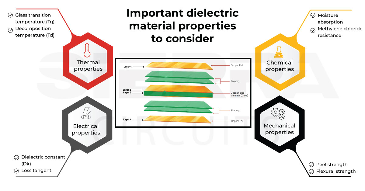
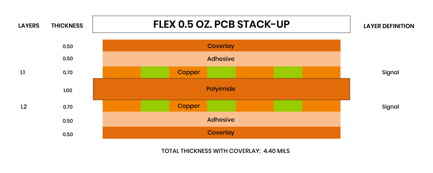
PCB Substrates: Knowing PCB Dielectric Materials

EasyEDA Std Tutorial
Layer - TARGET 3001! PCB Design Freeware is a Layout CAD Software
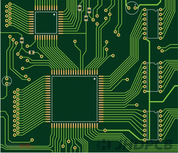
Best Guide To PCB Traces: Width, Thickness And Design Fix Recommendations - Jhdpcb
Epec's Blog Printed Circuit Boards (7)
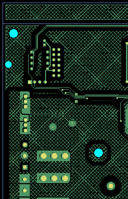
Copper balance - Multi Circuit Boards
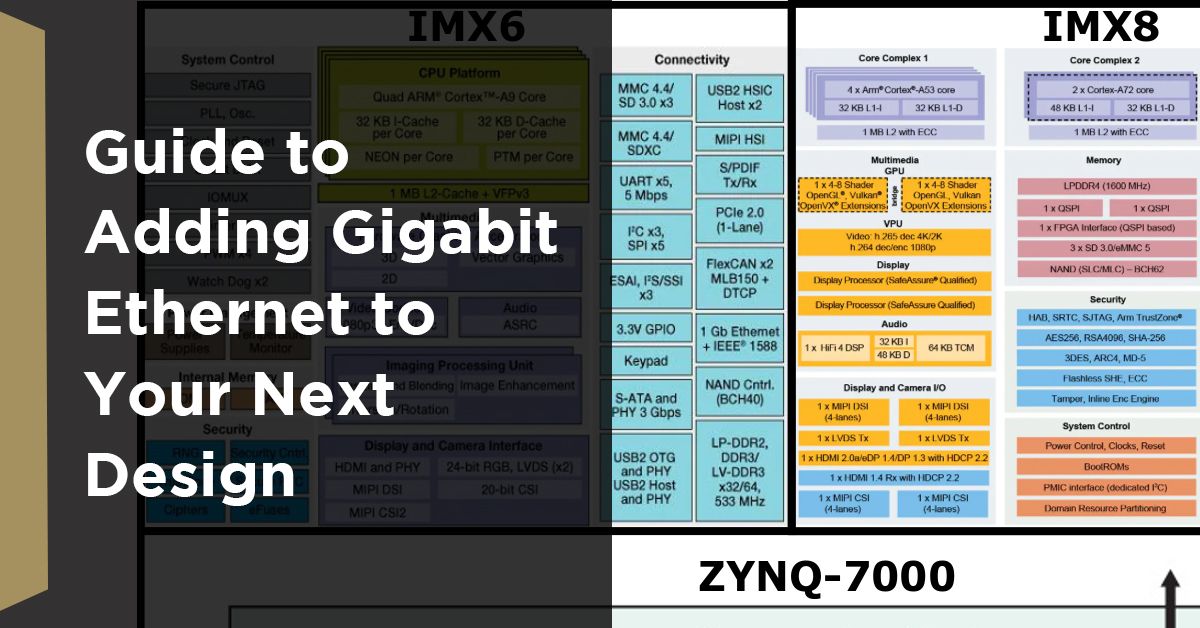
Gigabit Ethernet 101: Basics to Implementation, Blogs
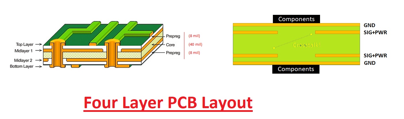
Four Layer PCB Layout: Design Process and Cost of Manufacturing
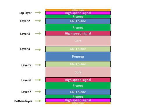
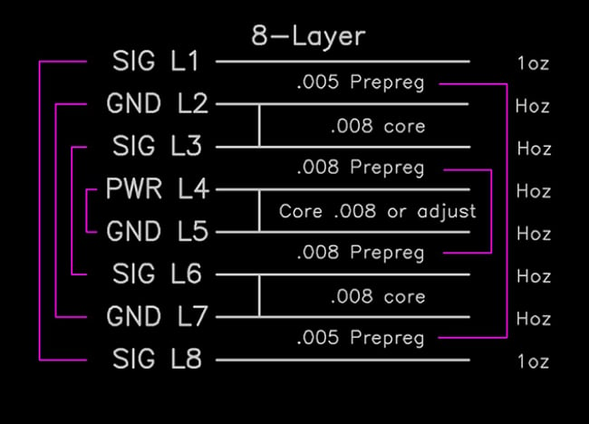
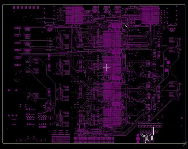
PCB Layer stack-up