The outline of bump bond process steps. (1) deposition of field
4.9 (598) · $ 7.99 · In stock

numerical method
Outline functional block diagram of the ESA ROIC front end-one pixel

Development of an Indium bump bond process for silicon pixel detectors at PSI - ScienceDirect

Hans ANDERSSON, Principal Research Engineer

Binder jet 3D printing—Process parameters, materials, properties, modeling, and challenges - ScienceDirect
The outline of bump bond process steps. (1) deposition of field metal

Left) A 64 x 64 pixel GaAs array produced to qualify the bump bonding
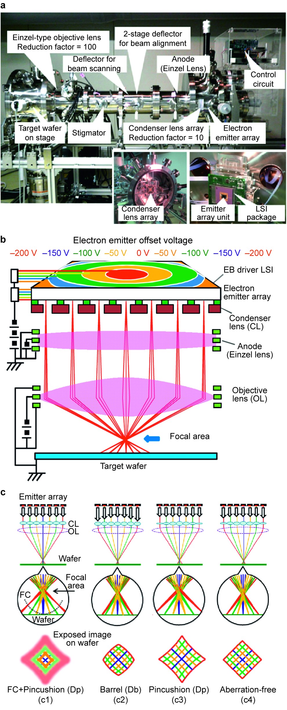
Development of massively parallel electron beam direct write lithography using active-matrix nanocrystalline-silicon electron emitter arrays
PPT - Surface micromachining and Process flow part 1 PowerPoint Presentation - ID:1589712

In-situ thermal control-assisted laser directed energy deposition of curved-surface thin-walled parts - ScienceDirect

Left) X-ray image of a line pair rule taken using an un-collimated

The outline of bump bond process steps. (1) deposition of field metal

Copper-to-copper direct bonding on highly (111)-oriented nanotwinned copper in no-vacuum ambient